

Ready-to-use semiconductor testing setups reduce calibration time and help researchers achieve consistent results from prototype to production.
Testing new semiconductor devices like silicon carbide (SiC) and gallium nitride (GaN) often requires complicated setups that take time to build and calibrate. Engineers and researchers need accurate results while testing to design reliable products.
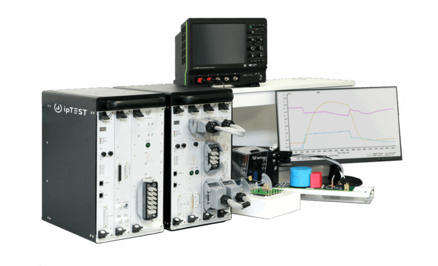
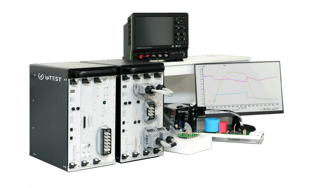
The Microtest Group launches two new testing systems: Quasar200 and Pulsar600 , these test tools solve the problem with complicated setup with plug-and-play, which lets users start testing power semiconductor devices without building custom test rigs or doing complex wiring. This helps labs and engineers save time while collecting reliable, repeatable data.
The Quasar200 is designed for testing standard and mid-range power semiconductor devices made from silicon (Si), gallium nitride (GaN), and silicon carbide (SiC). It focuses on precise DC and AC measurements, making it suitable for laboratory research, device characterisation, and datasheet development.
The Pulsar600 is built for high-current and high-power testing, particularly for SiC-based inverters and automotive systems. It supports short-circuit and stress tests up to 1,000 A DC and over 10,000 A AC, helping engineers validate the performance and safety of next-generation power modules used in electric vehicles and industrial applications.
The systems measure how semiconductor devices perform under high current and voltage. Quasar200 is built for testing silicon, GaN, and SiC devices used in electronics and power systems. It performs fast and accurate DC and AC measurements with low interference. Pulsar600 extends this capability to very high current applications, such as automotive and inverter testing, handling up to 1,000 amps DC and over 10,000 amps AC.
Both systems keep detailed audit logs for tracking data accuracy. This allows researchers and companies to match lab results with factory-level production tests when developing datasheets or qualifying new devices.
Safety is built into both systems. They include enclosed testing areas and ipTEST’s SocketSafe protection, which isolates power when equipment is opened or faults occur. Low-inductance sockets reduce electrical noise, improving test stability.
Key features
- Plug-and-play setup: Ready-to-use testing systems that remove the need for custom-built rigs or soldered connections.
- Wide device support: Compatible with silicon (Si), gallium nitride (GaN), and silicon carbide (SiC) devices.
- High current capability: Supports ultra-high current tests up to 1,000 A DC and 10,000 A+ AC, suitable for SiC inverters and automotive systems.
- Measurement precision: ±0.1% accuracy across all voltage and current waveforms.