


This new microchip process with precise materials and lasers allows making circuits smaller and more efficient.

While chips are being built at 3nm or smaller, not all chip components require extreme miniaturisation. Many interconnect layers, memory structures, or RF elements still use features in the 100–250nm range. It enables low-cost, scalable lithography for IoT MCUs, MEMS, or analog-digital mixed signal chips.
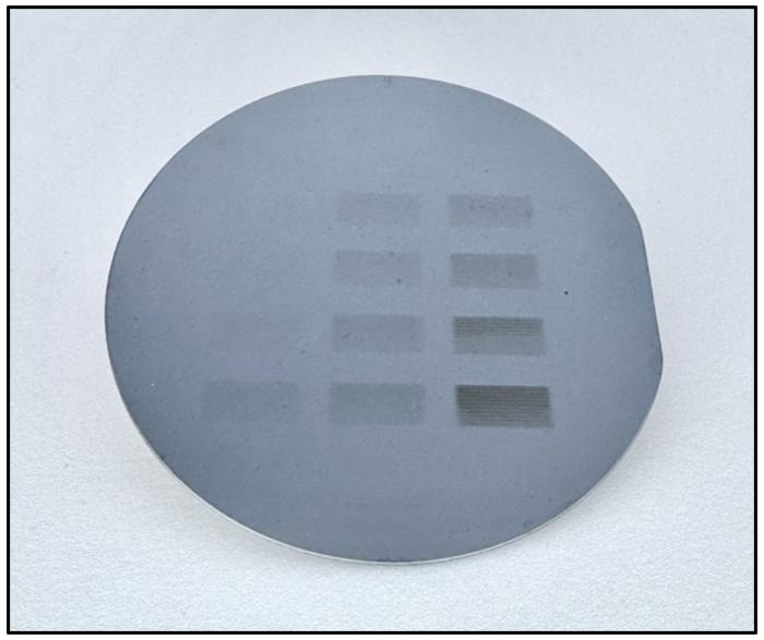
Johns Hopkins University researchers have introduced a fabrication process that enables circuit patterning on microchips at a precision of 229 nanometres. The method combines solution-based deposition techniques with new metal-organic resist materials, designed to function under next-generation laser lithography systems.
The process allows circuits to be written on silicon wafers using a method that relies on radiation-triggered reactions within a resist layer. This Resist layer above the silicon wafer is engineered from imidazole-based metal-organic compounds and responds to beyond extreme ultraviolet (B-EUV) radiation. B-EUV is a higher-energy successor to current EUV technology and is expected to be integrated into semiconductor manufacturing over the next decade.
Traditional Resists used in extreme ultraviolet lithography degrade under the intense energy levels required for such fine-scale patterning. In contrast, the resists developed by the Johns Hopkins team are designed to absorb B-EUV radiation more efficiently, particularly when paired with metals like zinc. When irradiated, these metals emit electrons that initiate chemical changes in the imidazole, the resist layer on silicon wafer forming precise circuit patterns.
The resist material is deposited via chemical liquid deposition (CLD), allowing engineers to tune thickness with nanometre accuracy. This control is essential for chip manufacturers aiming to increase transistor density while maintaining manufacturability and cost efficiency.
By enabling scalable, high-resolution lithography with adaptable material chemistry, the method addresses a key bottleneck in subwavelength chip fabrication.