


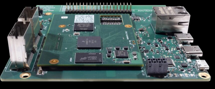
It uses physics-driven AI to automate PCB placement, routing, and validation, giving engineers more layout options while keeping control over constraints and final design decisions.
Designing a PCB is not simply about connecting one component to another. Engineers have to decide where components should sit, how signals should travel, how differential pairs and impedance-controlled nets should be routed, where power and ground should go, and how the board will behave within its mechanical and manufacturing constraints. For a simple board, these decisions can be handled manually. As component count, routing density, signal speeds, and design constraints increase, however, PCB layout can become one of the longest stages of hardware development.
Quilter approaches this problem differently from a conventional PCB autorouter. It uses physics-driven AI to automate component placement and routing and generate complete PCB layout candidates. Engineers provide an existing ECAD design, board outline, constraints, floorplan information, and other requirements. Quilter then analyses the design and produces multiple placement-and-routing candidates while applying design and physics constraints during generation. The output can be returned to the engineer’s existing ECAD environment rather than forcing a completely new PCB design workflow. It currently supports workflows involving Altium, Cadence, Siemens Xpedition, and KiCad.
What Does Quilter Actually Do?
The easiest way to understand Quilter is to think of it as an automated PCB layout engineer working alongside the human designer. Instead of manually placing hundreds of components and then routing thousands of connections, the engineer gives Quilter the electrical design and defines what must not be violated. The system then explores possible physical implementations. This distinction matters because Quilter is not intended simply to find a path between two pins. Its approach is to consider electrical and physical characteristics while generating the board. Engineers can use it to:
- Generate component placement automatically.
- Route PCB connections automatically.
- Generate multiple complete layout candidates.
- Work with differential pairs and impedance-controlled signals.
- Account for stackup information during routing.
- Respect placement regions and keepouts.
- Generate BGA fanouts and breakout routing.
- Apply manufacturing-related constraints.
- Compare different floorplans and stackup possibilities.
- Iterate on a design without manually rebuilding the entire layout.
The objective is therefore not necessarily to produce one “correct” layout. It is to give engineers several viable implementations so they can evaluate trade-offs and select or refine the design that best fits the product.
How Does It Help a PCB Engineer?
The biggest potential benefit is time spent exploring design alternatives. In a conventional workflow, an engineer may spend substantial time getting the first complete placement and routing into shape. If the resulting layout has problems, changing the floorplan, component positions or stackup can require significant manual rework. Quilter changes that equation by allowing engineers to generate and compare alternatives. Its pricing page also says users can run multiple jobs in parallel, such as different stackups, floorplans or trace-width choices.
This can be particularly useful during early hardware development. An engineer could, for example, investigate whether a board is better served by a different layer stackup or component arrangement before committing large amounts of manual layout effort. The tool is also designed to work with partially completed boards. Engineers can retain particularly sensitive sections, such as RF or high-voltage routing, before uploading the remainder. Quilter says already-routed pins do not count toward the project’s pin-count pricing and that it can route around existing work. That makes the tool potentially more useful as an engineering assistant than as a simple “upload everything and walk away” system. One design engineer mentioned that “We cut four weeks off bring-up on an 8-layer board and hit a holiday build we thought we’d miss. Our designers are still using Altium for final polish, but Quilter does the heavy lifting. It’s a force multiplier.”
What Does an Engineer Need Before Using Quilter?
Quilter does not remove the need for design preparation. The quality of the input still matters. A practical workflow looks like this:
1. Prepare the electrical design
The engineer begins with a schematic and associated PCB information in a supported ECAD environment.
2. Define the board
The board outline, component requirements and other physical restrictions need to be established.
3. Define design intent
Critical components, connectors, placement regions, keepouts and other requirements should be communicated before automated layout begins.
4. Check the stackup
Layer structure and material information are important for impedance-controlled routing. Quilter’s newer releases can import stackup information from input files and expose more stackup and fabrication parameters during setup.
5. Identify sensitive circuitry
An engineer may choose to retain control over RF, high-voltage or otherwise sensitive portions of a board rather than asking automation to handle every section.
6. Submit the design
Quilter analyses the design and generates layout candidates.
7. Review the candidates
The engineer remains responsible for deciding whether a candidate actually makes engineering sense. Rule compliance alone should not be treated as proof that a board is ready for production.
8. Iterate
If the result is not satisfactory, the engineer can change placement intent, stackup or constraints and generate another candidate.
This iterative approach is central to Quilter. The company says most customers iterate multiple times before going to fabrication and its project system groups those iterations together. Key Features Engineers Should Know
- Physics-driven placement and routing — considers electrical and physical constraints during layout generation.
- Multiple design candidates — allows engineers to explore alternatives instead of accepting a single routing result.
- Stackup-aware impedance control — uses stackup material information to calculate routing geometry.
- Differential-pair support — handles impedance-controlled differential signals.
- Automated BGA fanout — removes a previously manual preparation step for supported BGA patterns.
- Placement regions and clustering — lets engineers communicate placement intent.
- Keepout support — useful for mechanical, RF and sensitive-area restrictions.
- Native ECAD output — returns designs to supported ECAD environments.
- Unlimited project iterations — according to Quilter’s commercial pricing model.
- Parallel design exploration — enables different design configurations to be evaluated simultaneously.
What Is New?
The most important changes have arrived during 2026. Instead of adding only interface improvements, Quilter has been expanding the types of engineering information it can understand and use during layout.
Automated BGA Fanout One of the most significant additions is automated BGA fanout. Previously, engineers using Quilter had to perform BGA fanout manually in their ECAD software before submitting a dense board. The newer system can generate fanout and breakout routing as part of candidate generation.
This is important because BGAs can contain hundreds or thousands of connections concentrated underneath a single package. Fanout is often one of the first major manual layout tasks on a dense board. Quilter’s 2026 implementation selects via patterns, escape directions and breakout routing based on the stackup and surrounding board layout. “The win isn’t just speed. It’s the parallelism. I get multiple viable layouts to choose from, with the physics checks already done. That changes how we plan the entire program”, an electronic engineer mentioned.
- Calculated Impedance Profiles:Another important development is calculated impedance control. Quilter can calculate impedance profiles for differential-pair and single-ended impedance-controlled signals across board layers using the stackup material information. The calculations use the Simbeor solver from Simberian. For an engineer, the important change is that impedance is becoming part of the automated routing process rather than something that has to be approximated separately. The June 2026 update also allows engineers to enter their own differential-pair impedance values rather than being limited to predefined values.
- Placement Regions and Smart Clustering:March 2026 introduced placement regions and smart clustering. An engineer can define areas in which components should remain together, isolated, or local to a particular portion of the board. Quilter can also identify components that are directly connected in the schematic and cluster them during placement. An anchoring function allows an engineer to position one component while keeping the associated cluster together. This is important because automated placement becomes much more useful when the engineer can communicate why components belong in particular locations, rather than simply allowing an algorithm to optimise the board geometrically.
- Stackup and Keepout Awareness:Quilter has also moved toward importing more design intent directly from ECAD files. Stackup information can be imported from the input design, while keepouts can be used as first-class constraints for traces, vias, components and copper pours. These can be used for applications such as protecting antennas, reserving mechanical space or preventing routing underneath sensitive ICs.
- Clearance Constraints: Clearance-constraint support entered beta in May 2026. For supported Altium inputs, Quilter can read net-class, layer-specific and pair-specific clearance rules and apply them during placement and routing. This is significant because the more accurately an automated system understands the engineer’s existing constraints, the less work is required to translate design intent manually into the automation platform.
What Is Coming Next?
One of the most important developments to watch is blind and buried via support. Quilter says this capability is in active development. At present, its routing supports through-vias, while blind and buried vias are intended to extend the platform toward HDI and other dense designs that rely on multi-tier via structures. For engineers working on advanced compact electronics, this could be a particularly important milestone because HDI designs can require significantly more sophisticated physical implementation.
Is There a Free Version?
Yes. This is one of the most interesting aspects for engineers who want to experiment with AI-based PCB layout. Quilter currently offers a free tier for personal and academic use, with eligibility also extending to certain exploratory R&D situations. The company describes the free version as using the same physics-driven layout engine rather than a separate stripped-down “lite” engine. However, there is an important consideration for engineers working with proprietary designs.
Quilter states that designs submitted through the free offering may be used to generate synthetic training data for improving its AI. For commercial work where design confidentiality is important, Quilter directs users toward its commercial offering. This means the free version is best viewed as a learning, experimentation and evaluation environment, not automatically as the right place for confidential product designs. For commercial projects, Quilter uses a pay-per-project model rather than a traditional per-seat annual licence. Pricing is based on the number of pins that need to be routed. Engineers can also pre-route portions of a board and have Quilter work around that existing design. Commercial projects include unlimited iterations, according to the current pricing information. Commercial deployment can be through Quilter’s managed cloud or a self-hosted environment. The company says its cloud offering is SOC 2 Type 2 compliant, while self-hosting keeps the data within the customer’s infrastructure.
Quilter vs Traditional PCB Autorouting
The distinction is important. A conventional autorouter generally works within a PCB that has already been substantially defined by the engineer. Components are placed, design rules are established and the autorouter attempts to connect the remaining nets. Quilter is aiming at a larger part of the problem: placement + routing + physics validation. Its system can generate multiple complete layout candidates and evaluate them against constraints during generation. The company positions this as different from conventional geometric maze-solving and from generic AI systems that simply manipulate design data.
For an engineer, the practical question is therefore not “Can it draw traces?” Most PCB tools can do that. The more interesting question is: Can it explore a sufficiently large part of the physical design space while respecting the engineering constraints that matter to my board? That is where Quilter’s development is worth watching.
Advantages
- Can automate placement and routing together.
- Generates multiple layout alternatives.
- Useful for exploring different stackups and floorplans.
- Increasingly understands constraints directly from ECAD files.
- Supports impedance-controlled routing.
- Automated BGA fanout reduces manual preparation.
- Can work around engineer-routed sections.
- Returns output to supported ECAD environments.
- Free version allows engineers to experiment on suitable non-confidential designs.
- Commercial projects support repeated iterations.
Limitations
- It is still an evolving technology.
- Engineers must review generated layouts rather than assuming automatic routing means production readiness.
- Advanced design types may not yet be fully supported.
- Blind and buried vias are still under development.
- Some constraint support is still being expanded.
- Free-tier confidentiality considerations make it unsuitable for many proprietary commercial designs.
- Engineers new to AI-assisted PCB design may need to learn how to communicate design intent effectively.
Who Should Try Quilter?
Quilter is particularly interesting for engineers who regularly face PCB layout bottlenecks. PCB designers can use it to automate repetitive placement and routing work while retaining control over important areas.
Electrical engineers can use it to investigate how their schematic translates into different physical implementations. High-speed designers may find the impedance and differential-pair capabilities useful when exploring alternative layouts. Hardware startups can use the automation to investigate more board configurations without expanding the layout team for every iteration.
Students and researchers can experiment with AI-driven PCB design through the free offering, provided they use suitable non-confidential projects. Experienced engineers may find the biggest value not in replacing their expertise but in using automation to explore possibilities that would otherwise take too long to investigate manually.
For someone learning PCB design from scratch, Quilter should probably not be the only tool they learn. Understanding schematic capture, component libraries, placement, routing, stackups, impedance, signal integrity, power distribution, DRC, manufacturing constraints and mechanical integration remains important. But that is also why Quilter is interesting for engineers.
The tool represents a shift from “the engineer draws the PCB and the software helps” toward “the engineer defines the engineering problem and the software explores possible physical solutions.” The most exciting part is therefore not simply automatic routing. It is the growing ability to encode engineering intent—placement regions, keepouts, stackups, impedance requirements, clearance rules, BGA fanout and other constraints—and have the system use that information while generating the board. For engineers, this can change where time is spent. Instead of spending the majority of the layout cycle manually connecting every net, more time can be devoted to deciding what the board should achieve, comparing alternative implementations, reviewing the generated solutions and improving the design itself.
That is the real promise of physics-driven AI in EDA: not removing the engineer from PCB design, but giving the engineer more design space to work with. Quilter is not yet a reason to discard an existing ECAD workflow. It is more useful to think of it as an additional engineering capability that can automate one of the most time-consuming parts of hardware development. As support for more complex constraints, HDI structures and advanced board technologies expands, its usefulness to professional PCB designers is likely to become clearer.
For more information, click here.