


Scientists integrate atom-thin memory into traditional silicon, opening a new frontier in chip design.
In a major leap for semiconductor innovation, researchers have developed the world’s first fully functional memory chip that merges two-dimensional (2D) materials—just a few atoms thick—with conventional silicon circuitry. The achievement marks a pivotal moment in overcoming the miniaturization limits of today’s silicon-based technology.
For decades, engineers have pushed silicon to its physical boundaries, shrinking transistors to near-atomic scales. As performance gains flatten, the semiconductor industry has turned to 2D materials—like graphene and transition metal dichalcogenides—that offer exceptional electronic properties at atomic thicknesses. Yet integrating them into mainstream silicon chips has remained a formidable challenge.
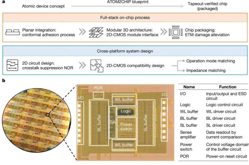
Now, scientists led by Chunsen Liu at Fudan University have cracked the problem. Using a novel technique dubbed ATOM2CHIP, the team successfully grew atomically thin 2D memory cells directly atop conventional silicon. The result is a hybrid chip that unites the speed, scalability, and low-power benefits of 2D materials with the maturity and robustness of silicon manufacturing.
Published in Nature, the study describes how the ATOM2CHIP process ensures stable electrical contact between ultra-thin 2D layers and thicker silicon circuits—long a stumbling block in the field. The researchers also devised a specialized packaging approach to shield the delicate layers from heat, stress, and static interference.
The team’s prototype isn’t just a lab experiment—it’s a fully operational chip, tested at 5 MHz and verified through “checkerboard programming” to confirm system-wide reliability. It demonstrates faster operation and dramatically lower energy use compared to conventional silicon memory.
Experts say the implications could be profound. This hybrid 2D–silicon architecture could redefine data storage and computing performance, enabling faster, smaller, and more efficient chips for next-generation artificial intelligence and mobile devices.As silicon nears its scaling limits, this breakthrough suggests a clear path forward—one where atom-thin materials seamlessly extend the life and capabilities of traditional chip technology, ushering in a new era of computing innovation.