


The low-cost method adds high-speed GaN transistors directly to standard silicon chips for better performance and easy scaling.

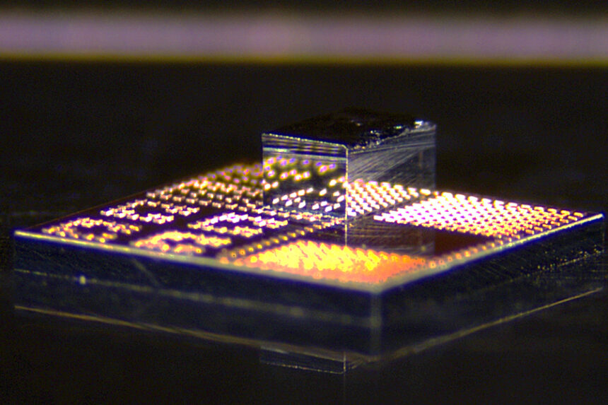
Researchers at MIT and partner institutions have developed a new process to integrate gallium nitride (GaN) transistors onto standard silicon CMOS chips. The process fabricates dense arrays of ultra-small GaN transistors—each only 240 by 410 microns—on a GaN wafer. These are then laser-cut into individual dielets.
Each dielet includes copper pillars that bond directly to matching copper features on a CMOS chip. A custom-built assembly tool aligns the dielets using vacuum control and nanometer-scale positioning before bonding at temperatures below 400°C.

Unlike traditional methods that require solder or gold bonding, this approach uses copper-to-copper bonding, which is more compatible with standard semiconductor fabrication environments.
The researchers demonstrated this technique by building power amplifier chips on Intel 22nm FinFET-based silicon, showing how GaN transistors can be added to advanced digital platforms.
This process eliminates the need to bond an entire GaN wafer to silicon, significantly reducing GaN material usage. Only the necessary transistors are transferred, minimizing waste and lowering material costs.
Copper bonding at low temperatures avoids thermal damage to sensitive components and does not require expensive materials like gold, which also pose contamination risks in standard fabs.
The method supports high-density integration of GaN transistors with advanced silicon nodes, allowing the use of additional circuit elements like neutralization capacitors that improve RF performance.
By fitting within existing chip manufacturing workflows, the technique enables easier scaling and commercial adoption without major changes to fabrication infrastructure.
The resulting chips are smaller, faster, and more efficient. Power amplifiers made using this method deliver higher bandwidth and stronger signal gain compared to those made with silicon alone.
This integration technique could lead to improved wireless connectivity, longer battery life in mobile devices, and more compact hardware design.
Because GaN performs better than silicon at low temperatures, the same method could support emerging applications such as cryogenic electronics and quantum computing.
By bridging the strengths of GaN and silicon in a low-cost, scalable way, the technology opens new possibilities for high-performance systems—from mobile phones to AI and next-generation communication infrastructure.