


JOB: PCB Librarian And Component Engineer At Astrome In Bengaluru
APPLY HERE ON LINKEDIN Location: Bengaluru Company: Astrome About the Job Requirements

PCB Layout Engineer II At OSI Systems In Hyderabad
Location: Hyderabad Company: OSI Systems PCB layout engineer will design multi layer…

A Unified EDA Platform For Smarter PCB Development
Explore how this all-in-one PCB design and EDA tool helps engineers go…


A Practical EDA Tool for Modern PCB Engineering
Engineers can take advantage of faster routing, improved workflow tools, and enhanced…

JOB: PCB Layout Engineer At Sanmina In Chennai
APPLY HERE Location: Chennai Company: Sanmina Duties of Position: (Include specific duties…

Electronics Assembly & Soldering Technician At PCB CUPID In Bengaluru
Location: Peenya 2nd Stage, Bengaluru, Karnataka 560058 Company: PCB CUPID Role Responsibilities…
JOB: PCB Design Engineer At Sanmina In Chennai
APPLY HERE Location: Chennai Company: Sanmina Duties of Position: (Include specific duties…
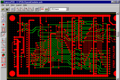
Free Windows-Based PCB Designing Tool
- Advertisement - Want a PCB design tool from designing to manufacturing?…